|
|
Photonic Crystals

The periodic arrangement of ions on a lattice gives rise to the energy band structure in semiconductors. Energy bands control the motion of charge carriers through the crystal. Similarly, in a photonic crystal, the periodic arrangement of refractive index variation, controls how photons are able to move through the crystal.
Replacing the ions on a lattice are regions of low refractive index within a
high-refractive index material or vice-versa. Photons react to the refractive
index contrast in an analogous manner to the way electrons react when
confronted with a periodic potential of ions. Each results in a range of
allowed energies and a band structure characterised by an energy gap or
photonic band gap. A band gap forms when the electron wavelength is comparable
to the inter-atomic spacing.
Photonic band gaps were first predicted in 1987 by two physicists working
independently. They were Eli Yablonovitch, at Bell Communications Research in
Red Bank, New Jersey, and Sajeev John of the University of Toronto. An array of
1mm holes milled into a slab of material of refractive index 3.6, latter to
be known as Yablonovite, was found to prevent microwaves from propagating in
any direction. An estimate of the distance between voids is given by the
wavelength of the light divided by the refractive index of the material. This
relationship means that it is even more difficult to create photonic crystals
in materials with high refractive index. Finding materials and techniques of
producing photonic crystals has remained illusive until 1997.
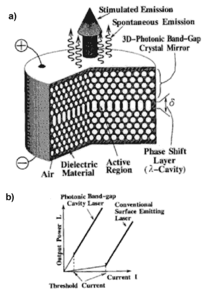
Breaking the periodicity of the voids in the photonic crystal, either by enlarging or reducing the size of a few of the voids, introduces new energy levels within the photonic band gap. This is analogous to the creation of energy levels within the band gap by the addition of dopant atoms in semiconductor crystals. Narrow line width lasers [1], that are so important in the area of Dense Wavelength Division Multiplexing (DWDM) communication systems, can be fabricated using photonic crystals formed from the III-V semiconductors or rare-earth doped glass. The defect mode or microcavities formed by breaking the periodicity of the crystal amplify only those wavelengths of light that are able to pass freely through the crystal. The wavelength range of emission is related to the diameter of the microcavity divided by the diameter of the regular holes. Photonic crystal microcavities are more efficient than conventional semiconductor diode lasers since there are few directions in the which the photons can escape.
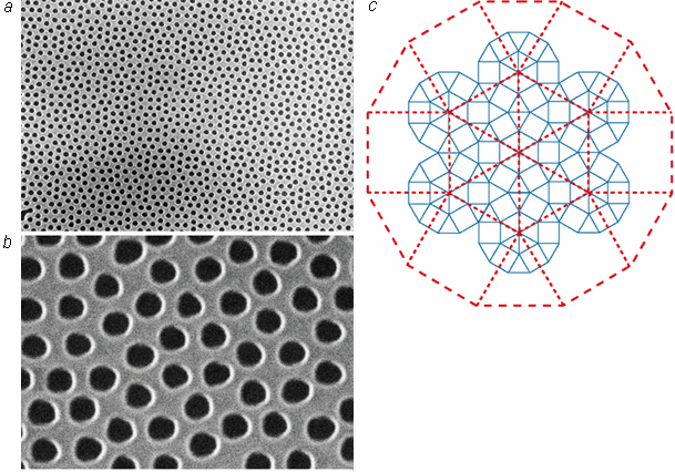
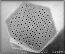
In passive devices, such as optical filters, where it is often required to filter a weak signal, the aim is to minimise further loss. Unfortunately, these losses are greater in materials with a high refractive index and photonic crystals use the contrast in refractive index to create energy band gaps. Altering the geometry of the voids, in such a way as to increase the symmetry of the periodic structure, the band gap can be restored in a low refractive index material. For example, by going from a rectangular array of voids in which the spacing of the holes is different for the two perpendicular directions within the plane, to a triangular arrangement which has a sixfold degree of symmetry within the plane. A quasiperiodic arrangement of holes have a photonic band gap what ever the angle of the light travels.
Source: IOP publications
Photonic crystals are also being exploited in the technology of optical fibres by Phillip Russell and Jonathan Knight et Al. at the University of Bath to create fibres that are carry light at high powers. Traditional optical fibres have a glass core surrounded by a cladding layer. The cladding has a lower refractive index than the core. The difference in the refractive index between the two materials is slight, but it is enough to cause light within the core to be reflected along the core by total internal reflection. At high powers, the light is concentrated in a very small region of space. Raman scattering can result, causing the light signal to be corrupted and at high powers the fibre can even be damaged.
The first photonic crystal fibres used a hexagonal array of air holes running the entire length of the fibre. The light travelled close to the fibre axis and so the power was still limited. By removing the central tubes to leave a central hole of 15 m m in diameter. The hole acts as a waveguide, the light being trapped by the photonic crystal structure around the hole. The photonic crystal allows only some of the light to propagate along the fibre.
Photonic crystal fibre is made by stacking pure silica tubes in a hexagonal array, and then heating and stretching it. This reduces the width of the structure, while retaining the geometry.
Ultimately, Professor Russell sees hollow-core fibres as the basis of ultra high-power fibre-delivery systems, in which light from a powerful laser source is delivered to a cutting head in surgery and machining. And one day soon, hollow-core fibre might guide atoms or particles over long distrances, forming the basis of fibre-optic devices that move matter.