|
|
Semiconductor Fabrication: Photolithography
Photolithography, literally meaning light-stone-writing in Greek, is the process by which patterns on a semiconductor material can be defined using light. It is the means by which the small-scale features of integrated circuits are created. The description that follows is by no means an exhaustive description of the process of photolithography and the reader is referred to the excellent introduction by R. B. Darling [1] for a fuller grounding on this topic.
Before the resist is applied to the substrate, the surface is cleaned to remove any traces of contamination from the surface of the wafer such as dust, organic, ionic and metallic compounds and a layer of Silicon dioxide is formed by a wet or dry oxidation process. The cleaned wafer is subject to priming, to aid the adhesion of the resist to the surface of the substrate material.
A resist is applied to the surface using a spin-coating machine. This device holds the wafer of semiconductor, using a vacuum, and spins it at high-speed (3000-6000 rpm) for a period of 15-30 seconds. A small quantity resist is dispensed in the centre of the spinning wafer. The rotation causes the resist to be spread across the surface of the wafer with excess being thrown spun off. Close to the centre of the wafer, the variation in the thickness of resist is around 30 nm. Preparation of the resist is concluded by a pre-bake, where the wafer is a gently heated in a convection oven and then a hotplate to evaporate the resist solvent and to partially solidify the resist.
The photomask is created by a photographic process and developed onto a glass substrate. The cheapest masks use ordinary photographic emulsion on soda lime glass, while Chrome on quartz glass is used for the high-resolution deep UV lithography.
Alignment of the mask is critical and must be achieved in for x-y as well as rotationally. Industrial photolithography machines use automatic pattern recognition to achieve the registration alignment.
Depending on the design of the photolithography machine, the mask may be in contact with the surface, very close to the surface or used to project the mask onto the surface of the substrate. These methods are called, not surprisingly, contact, proximity and projection respectively. Figure 1, shows a schematic diagram of these methods. The projection system is the most complex method but does mean the projection of the mask can be scaled. The limit of the feature size is limited by the diffraction limit and depends on the size of the wavelength of light used to illuminate the mask. Systems using UV light are limited to feature sizes of 1 &#mu;m.
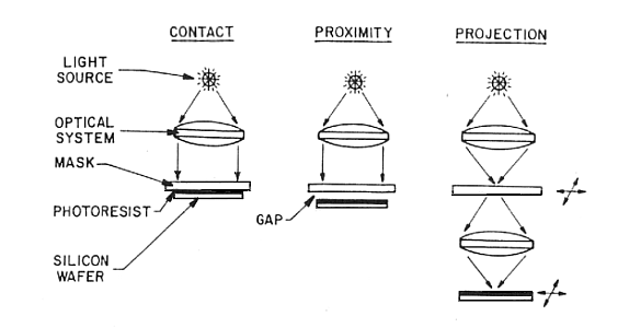
Figure 1. Contact, proximity and projection methods of photolithography.
An alternative to using a mask, is to directly expose the resist using an excimer laser, electron beam or ion beam. These systems do not require a mask. Such methods are known as Direct Write to Wafer methods (DWW). With the density of features steadily increasing keeping up with Moores law, finer lithographic techniques will be required.
|
Method |
Feature Size ( &#mu; m) |
|
UV Photolithography |
1 |
|
Laser DWW |
1-2 |
|
Electron Beam |
0.25-0.1 [2] |
|
Ion Beam |
0.05-0.1 |
|
X-Ray Lithography |
<0.1 |
Table 1. Smallest feature size for lithographic techniques.
During the exposure process, the resist undergoes a chemical reaction. Depending on the chemical composition of resist, it can react in two ways when the light strikes the surface. The action of light on a positive resist causes it to become polymerised where it has been exposed to the light. A negative resist has the reverse property. Exposure to UV-light cause the resist to decompose. After the developing process, a negative of the mask remains as a pattern of resist. Although not necessary for all processing, to further harden and remove any residue of the developer, the wafer undergoes a post-bake process. During this process, the resist temperature can be controlled to cause a plastic flow of the resist which can be desirable for tailoring sidewall angles. After either, deposition of semiconductor layers or metal or etching down to selectively remove parts of the SiO 2 , the resist can be removed. For positive photoresists, accetone, trichloroethylene and phenol-based strippers may be used. While negative resists are generally removed using, Methyl Ethyl Ketone (MEK) or Methyl Isobutyl Ketone (MIBK). Figure 2, shows the process schematically using a proximity mask.
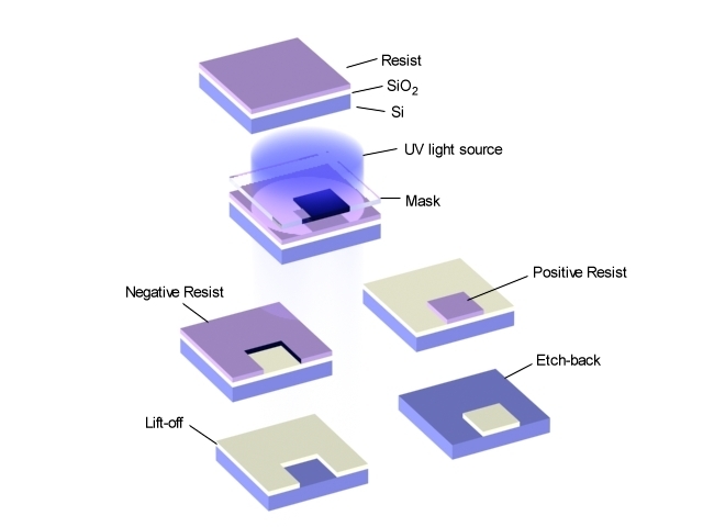
Figure 2. The main processes in the photolithography.
References:
[1] EE-527 Microfabrication, Photolitholgraphy, R. B. Darling.
[2] Mark. A. McCord, M. J. Rooks, SPIE HANDBOOK OF MICROLITHOGRAPHY,
MICROMACHINING AND MICROFABRICATION.
|
|